Task:
High resolution imaging of conductive and uncoated insulating sample surfaces, as well as high resolution materials modification and milling of nanostructures.
Specific information on the method:
- Lateral resolution: better than 0.4 nm (Helium, edge resolution)
- Imaging of insulating samples without any additional conductive coating.
- Helium and Neon implantation with energies up to 30 keV and 25 keV, respectively.
- Milling of nanostructures and polishing of cross section as well as TEM lamellas.
- Ion fluences up to 1×1024m-2
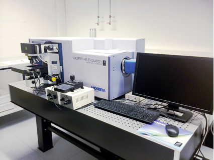
Specific information on the equipment/instrumentation:
Measurement in UHV (5×10⁻⁸ mbar), sample heating up to 500°C (in-preparation)
Samples/limitations:
Suitable for solids or powders, conductive samples as well as insulators, biological samples
Limitation: sample stable under UHV conditions, maximum size 50 mm, radiation damage at high magnifications.
Examples of typical imaging and nanomodification questions:
– High resolution imaging of nanowires or other 3D surfaces which require a large depth of focus.
– Visualization of conductive/isolating samples without any coating (i.e. metallic nanoparticles on insulating support)
– High resolution materials modification by Ne (He) implantation (such as implantation induced phase transformations)
– Milling of Ga free nanostructures with sizes smaller than in classic FIB processing.
– Ga free preparation of cross sections and lamella for TEM, SEM (EBSD, EDX) or HIM investigation.
Fields of research:
Materials for fuel cells, batteries, catalysis and electronic devices (e.g. transistors), high-T alloys, nuclear materials, ceramics, organic/inorganic compounds and polymers